1. Introduction
The rapid growth of artificial intelligence (AI) and data-intensive applications has exposed fundamental limits of conventional digital computing. The von Neumann architecture, which physically separates memory and processing units, incurs substantial energy and latency penalties from repeated data movement between them — a limitation widely referred to as the “memory wall.” Simultaneously, CMOS transistor scaling is approaching physical and economic limits, with rising leakage current, process variability, and thermal density constraints eroding the historical gains of Moore’s-law scaling.
Neuromorphic computing addresses these constraints by adopting brain-inspired design principles: memory and computation are co-located in neuron- and synapse-like elements, communication is event-driven (spike-based) rather than clocked, and local plasticity rules enable on-chip adaptation. In parallel, multi-valued logic (MVL) and multistate devices extend circuit elements beyond binary (0/1) representation to encode several discrete or continuous levels per device or interconnect, which can increase information density and reduce switching energy per unit of useful computation.
This paper unifies these two research strands. We argue that neuromorphic systems are natural beneficiaries of multistate device physics — particularly for synaptic weight storage and analog current accumulation — and that MVL circuit techniques can, in turn, be used to build compact and energy-efficient neuromorphic primitives such as multi-threshold neurons and carry-limited arithmetic units. The paper's contributions are:
- A structured review of neuromorphic computing fundamentals, representative large-scale chips, and their design principles.
- A device-physics-level analysis of four multistate device families — memristors/RRAM, ferroelectric FETs, spintronic elements, and hybrid molecular–semiconductor ternary transistors — and their suitability for neuromorphic functions.
- A quantitative hardware–algorithm co-design methodology that explicitly incorporates device variability, nonlinearity, and endurance constraints into model training, mapping, and evaluation.
- A synthesis of published energy and latency benchmarks for neuromorphic hardware, contextualized within the thermodynamic (Landauer) limits of computation.
- A near-, medium-, and long-term roadmap addressing standardization, tooling, and deployment challenges.
The remainder of the paper is organized as follows. Section 2 reviews background and related work. Section 3 examines the device physics of multistate elements. Section 4 discusses circuit- and system-level architectures. Section 5 covers algorithmic mappings. Section 6 presents the proposed co-design methodology in detail. Section 7 reports results and discussion, including benchmark synthesis and a reference-authenticity assessment. Section 8 presents a case study. Section 9 analyzes thermodynamic optimization opportunities. Sections 10–11 discuss open challenges and a research roadmap, Section 12 looks beyond the current state of the art to propose a predictive thermal-optimization framework and a set of future application domains, and Section 13 concludes.
2. Background and Related Work
2.1 Neuromorphic Computing Fundamentals
Neuromorphic engineering, pioneered by Carver Mead and Misha Mahowald in the late 1980s, builds analog and mixed-signal silicon circuits that emulate the dynamics of biological neurons and synapses, including early silicon retinas and cochleae. Contemporary neuromorphic systems most commonly implement Spiking Neural Networks (SNNs), in which neurons integrate synaptic input currents over time and emit discrete voltage “spikes” upon crossing a threshold, with information encoded in spike timing and rate rather than in a continuously valued activation.
Three properties distinguish neuromorphic systems from conventional accelerators:
- Event-driven operation: only neurons that receive sufficient input consume dynamic energy; inactive regions of the network draw near-zero current, in contrast to the static and clock-distribution power of synchronous digital logic.
- Massive, local parallelism: large numbers of neurons operate concurrently with locally stored state, reducing the volume of data that must move across the chip.
- Synaptic plasticity: connection weights can be updated in place via local learning rules such as spike-timing-dependent plasticity (STDP), enabling online and continual adaptation without returning to an external trainer.
Representative large-scale digital and mixed-signal neuromorphic chips include IBM TrueNorth and its successor NorthPole, Intel Loihi and Loihi 2, the University of Manchester's SpiNNaker digital multi-core mesh, and the Heidelberg BrainScaleS wafer-scale analog/mixed-signal system. These platforms differ substantially in neuron model fidelity, numeric precision, interconnect topology, and target application space, which complicates direct comparison (see Section 7.4).
2.2 Multi-Valued Logic and Multistate Devices
Binary logic dominates digital electronics because of its simplicity and noise margin robustness. Multi-valued logic (MVL) instead encodes more than two stable levels per device or wire — for example ternary (three-level) or quaternary (four-level) encodings — which can, in principle, reduce the number of physical devices and interconnects needed to represent a given amount of information, and can enable carry-limited arithmetic styles such as signed-digit and residue number representations. Reported demonstrations relevant to this review include ternary arithmetic circuits with favorable power-delay product (PDP) relative to binary counterparts in standard CMOS, hybrid silicon–zinc-oxide (ZnO) ternary transistors with a stable intermediate current plateau, and carbon-nanotube field-effect transistor (CNTFET) ternary gates.
MVL is of particular relevance to neuromorphic systems because biological synaptic weights are not binary: they vary continuously or over many discrete levels, and analog current accumulation across many synapses is central to how biological and neuromorphic networks compute.
2.3 Related Surveys and Positioning of This Work
Recent community surveys address neuromorphic computing at scale, robotic vision applications, continual learning on spiking hardware, and memristive device reliability. This paper differs from prior surveys in three respects: it explicitly couples the device-physics and algorithmic literatures around the shared theme of multistate representation; it proposes a structured, four-stage co-design methodology (Section 6) intended to be reproducible across device families; and it situates the resulting benchmark comparisons within an explicit thermodynamic accounting framework (Section 9), which is not commonly treated in neuromorphic hardware surveys.
3. Device Physics of Multistate Elements
The ability to sustain multiple stable, reproducible conductance or threshold-voltage levels in a single device underlies both multistate logic and analog neuromorphic synapses. We examine four device families relevant to current research.
3.1 Memristive Synapses (RRAM / CBRAM)
Resistive RAM (RRAM) and conductive-bridge RAM (CBRAM) devices change resistance through the formation and rupture of nanoscale conductive filaments (e.g., via migration of oxygen vacancies in an oxide layer) or through metal-ion migration between electrodes. Partial filament growth yields intermediate resistance states that support multi-bit, nonvolatile storage per cell, and repeated voltage pulsing can potentiate (lower resistance) or depress (raise resistance) the device in a manner that emulates synaptic plasticity. Principal engineering challenges include cycle-to-cycle and device-to-device variability, finite endurance under frequent updates, and nonlinear or asymmetric conductance-update behavior that complicates precise weight programming.
3.2 Ferroelectric Field-Effect Transistors (FeFETs)
FeFETs incorporate a ferroelectric layer within the gate stack whose polarization state sets the channel conductance. Partial domain switching enables several distinct threshold-voltage levels, supporting multi-bit synapse and neuron implementations. FeFETs are attractive for low write energy, fast polarization switching, and compatibility with conventional CMOS process flows, which eases large-scale integration relative to some emerging memory technologies.
3.3 Spintronic Devices (MTJs and Domain Walls)
Magnetic tunnel junctions (MTJs) and domain-wall devices exploit electron spin and magnetic texture to encode information. Multiple resistance states, or stochastic switching regimes, can emulate synaptic potentiation and depression, or probabilistic (“p-bit”) computation, while spin-torque oscillators and domain-wall motion can reproduce thresholding and refractory dynamics analogous to biological neurons. Magnetic states are inherently nonvolatile and comparatively tolerant to radiation, which is attractive for aerospace and other harsh-environment deployments, though integration complexity and specialized materials remain barriers to large-scale adoption.
3.4 Hybrid Molecular/Semiconductor Ternary Transistors
A further path to practical multistate logic uses hybrid silicon–ZnO transistors incorporating molecular linker layers. Alternating ZnO and molecular layers can produce a stable intermediate current plateau between the conventional OFF and ON states, enabling ternary (0/1/2) logic within a single transistor on a silicon-compatible process. The reported stability of the intermediate plateau across a range of gate voltages addresses a reliability limitation that constrained earlier MVL device proposals.
3.5 Comparative Summary of Device Families
Table 1 summarizes the four device families discussed above along the dimensions most relevant to neuromorphic and multistate circuit design: switching mechanism, typical number of stable states reported in the literature, nonvolatility, principal advantages, and principal open challenges.
| Device Family | Switching Mechanism | Typical States | Nonvolatile? | Key Advantage | Key Challenge |
|---|---|---|---|---|---|
| Memristor / RRAM / CBRAM | Filament formation/rupture; ion migration | 4–32+ (analog) | Yes | Dense, in-situ analog weight storage | Cycle-to-cycle variability, endurance limits |
| Ferroelectric FET (FeFET) | Ferroelectric domain polarization switching | 2–8 (multi-V_T) | Yes | Low write energy, CMOS-compatible | Variability at scaled nodes, retention |
| Spintronic (MTJ / domain wall) | Spin-torque switching; domain-wall motion | 2–4 (or stochastic) | Yes | Radiation tolerance, fast switching | Integration complexity, material stack |
| Hybrid molecular/ZnO ternary transistor | Quantized intermediate current plateau | 3 (ternary) | Depends on design | Silicon-compatible ternary logic | Manufacturing maturity, yield data limited |
4. Circuit and System Architectures
4.1 Neuromorphic Core with Multistate Synapses
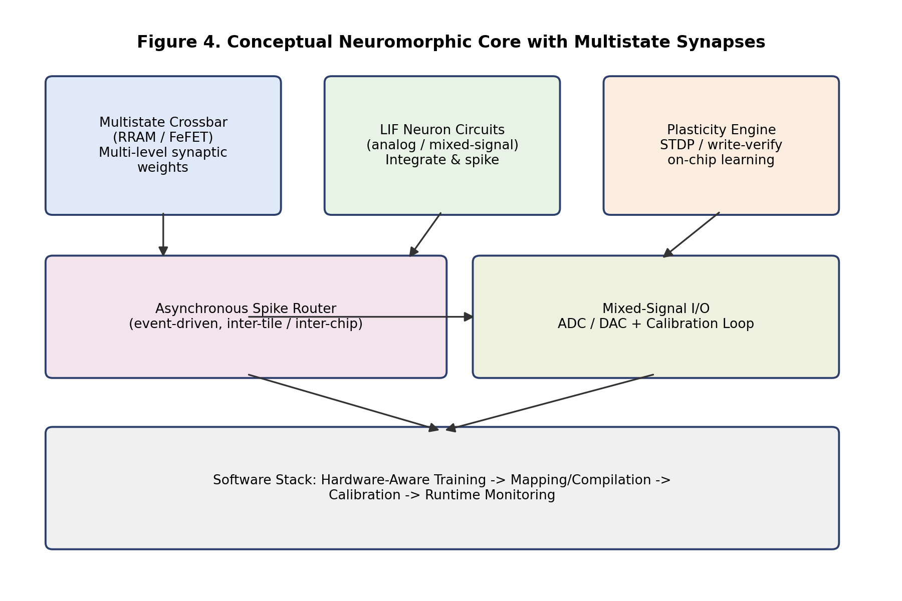
A representative neuromorphic core (Figure 4) comprises four principal blocks. Crossbar arrays of memristive or FeFET devices store synaptic weights as multi-level conductance and perform analog matrix–vector multiplication in place, using Ohm's law for multiplication and Kirchhoff's current law for summation at each column. Leaky integrate-and-fire (LIF) neuron circuits, implemented in analog or mixed-signal form, accumulate the resulting currents and emit spikes upon threshold crossing. A local plasticity engine adjusts device conductances based on spike timing or globally broadcast error signals, optionally using iterative write-and-verify pulses to compensate for device nonlinearity. Finally, an asynchronous, event-based spike router propagates spikes between cores or chips with minimal idle power. This architecture directly addresses the memory wall by co-locating weights and computation and by exploiting sparse, event-driven communication instead of a fixed clock.
4.2 Multistate Logic and Arithmetic
MVL circuits complement neuromorphic cores in two ways: by providing compact peripheral logic (e.g., ternary inverters, NAND/NOR, and cycling gates that can implement functions requiring multiple binary transistors in a single multistate device) and by enabling carry-limited arithmetic. Multi-valued representations such as signed-digit or residue number codes can bound carry-propagation length, enabling fast, highly parallel adders and multipliers suitable for neural accelerators and digital signal processing (DSP).
4.3 Mixed-Signal Integration and Calibration
Because crossbar accumulation and LIF integration are analog operations, practical systems require analog-to-digital and digital-to-analog converters (ADC/DAC) to interface with digital control and spike-routing logic. ADC energy and area overhead is frequently cited as a key bottleneck in analog in-memory computing, since converter cost scales unfavorably with the resolution needed to fully exploit multi-level device states. Device mismatch and non-ideal conductance behavior further necessitate per-device calibration, iterative parameter storage, or “chip-in-the-loop” training procedures, in which the physical hardware participates directly in the training loop so that the learned parameters already account for device-specific nonlinearity.
5. Algorithms and Mappings
5.1 Spiking Neural Networks (SNNs)
SNNs remain the canonical neuromorphic computational model. Static or temporal inputs are converted into spike trains by an encoder; LIF or related neuron models integrate weighted input spikes, apply a threshold, and enter a refractory period after firing; and local learning rules such as STDP adjust synaptic weights based on the relative timing of pre- and post-synaptic spikes. Because the discrete, non-differentiable spike-generation function is not directly compatible with standard backpropagation, direct SNN training typically relies on surrogate-gradient methods that substitute a smooth function for the spike derivative during the backward pass.
5.2 ANN-to-SNN Conversion and Multi-Level Networks
An alternative to direct SNN training is to train a conventional artificial neural network (ANN) and then convert it to a spiking equivalent by normalizing weights and activations so that firing rates approximate the original ANN activations. Separately, multistate hardware motivates networks with discrete multi-valued activations and weights (e.g., ternary or quaternary), which trade a controlled amount of numeric precision for substantial gains in energy and area by matching the network's native representation to the device's native conductance levels; quantization-aware training and knowledge distillation are commonly used to limit the resulting accuracy loss.
5.3 Continual and Online Learning
Neuromorphic systems are particularly well suited to resource-constrained, non-stationary environments. Neuromorphic continual learning (NCL) approaches combine SNN dynamics with continual-learning objectives — low catastrophic forgetting and low incremental compute/memory cost — for online adaptation, and hybrid schemes that combine unsupervised STDP-like plasticity with sparse supervised error signals have been proposed to balance adaptability against training stability.
6. Methodology: Hardware–Algorithm Co-Design Under Device Constraints
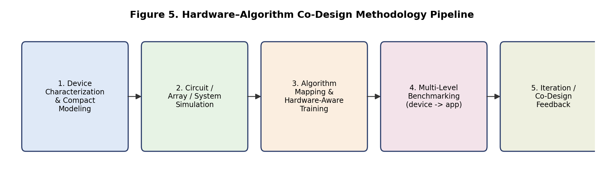
To evaluate neuromorphic–multistate systems in a way that is reproducible and comparable across device families, we propose a four-stage co-design methodology, illustrated in Figure 5: (1) device characterization and compact modeling, (2) circuit/array/system simulation, (3) algorithm mapping with hardware-aware training, and (4) multi-level benchmarking with an explicit feedback loop back to device and circuit design.
6.1 Device Characterization and Compact Modeling
- Fabrication and measurement. Target devices (memristors, FeFETs, ternary transistors) are fabricated or sourced, and key metrics are measured: number of stable states, switching energy per operation, switching latency, endurance (write/erase cycles to failure), retention time, and both cycle-to-cycle and device-to-device variability.
- Compact modeling. A physics-based or behavioral compact model is developed to capture nonlinear and asymmetric conductance updates, state-dependent switching dynamics, thermal sensitivity, stochastic noise, and long-term drift.
- Parameter extraction. Model parameters are fit to measurement data (e.g., via least-squares or maximum-likelihood estimation) for use in downstream circuit and system simulation.
6.2 Circuit and Architecture Simulation
- Circuit-level simulation. SPICE-class simulators evaluate neuron/synapse circuits using the extracted device models, reporting energy per spike or synaptic update, latency, and the impact of variability on neural dynamics.
- Array-level simulation. Crossbar arrays are simulated with realistic device-parameter distributions (drawn from the variability statistics in Section 6.1) to assess matrix–vector multiplication accuracy, usable dynamic range, ADC resolution requirements, and calibration overhead.
- System-level simulation. Cores, spike routers, and I/O interfaces are integrated in an architectural simulator to estimate throughput, energy per inference or per weight update, and scalability to larger networks.
6.3 Algorithm Mapping and Hardware-Aware Training
- Model selection. A target algorithm class (SNN, quantized multi-level network, or hybrid ANN–SNN) is chosen to match application requirements for latency, accuracy, and power.
- Hardware-aware training. Device constraints are incorporated directly into training: weights and activations are quantized to the number of levels the target device can reliably hold; conductance nonlinearity and variability are simulated during the forward pass; and regularization terms penalize solutions that are fragile to expected device drift.
- Mapping and compilation. The trained model is mapped onto physical hardware resources: neurons are assigned to cores, weight matrices are partitioned across crossbar arrays, spike/event schedules are generated, and plasticity-rule parameters are configured.
6.4 Multi-Level Benchmarking
We adopt a benchmark hierarchy spanning four levels, summarized in Table 2:
- Device level: endurance, retention, energy per switching event, and state-to-state variability.
- Circuit level: energy per event, latency, and power-delay product (PDP) for representative gates and arithmetic units.
- System level: energy per inference or per weight update, throughput, and end-to-end latency on standard and neuromorphic-specific workloads.
- Application level: accuracy–efficiency trade-offs on representative tasks such as event-based vision, keyword spotting, robotic control, and continual learning.
6.4.1 Formal Metric Definitions
For clarity and reproducibility, we define the core metrics used in Section 7 as follows. The power-delay product of a circuit is PDP = E_op, the energy dissipated per switching operation, computed as the time-integral of instantaneous power over one operation; lower PDP indicates a more efficient gate for a given technology node. Energy per inference is defined as the total electrical energy consumed by a system (including any necessary ADC/DAC and control overhead) divided by the number of inferences completed in that interval. Because published figures for different platforms are measured under different workloads, process nodes, and measurement boundaries (chip-only versus board-level, including or excluding I/O), we treat cross-platform comparisons in Section 7.1 as order-of-magnitude indicators rather than strictly controlled comparisons, and we recommend the standardized benchmark hierarchy above as a prerequisite for tighter comparison.
6.5 Threats to Validity
Several factors limit the strength of conclusions that can currently be drawn from cross-platform neuromorphic benchmarking, and we flag them explicitly rather than treating reported figures as directly comparable: (i) heterogeneous measurement boundaries (chip-only power versus full-system power, including or excluding host-CPU orchestration); (ii) workload mismatch, since neuromorphic-favorable benchmarks emphasize sparse, event-driven inputs while GPU/CPU baselines are typically reported on dense, batched workloads; (iii) process-node disparity, since some neuromorphic chips are fabricated at older nodes than the GPUs against which they are compared, which independently affects energy per operation; and (iv) self-reported vendor figures that have not always been independently reproduced. These limitations motivate the standardized, multi-level benchmark suite proposed above.
| Level | Representative Metrics | Typical Tooling |
|---|---|---|
| Device | Endurance (cycles), retention (s–years), energy/switch (aJ–fJ), state variability (%) | Parameter analyzers, pulsed I–V measurement |
| Circuit | Energy/event, latency, power-delay product (PDP) | SPICE-class circuit simulation |
| System | Energy/inference, throughput (inf/s), scalability | Architectural / cycle-level simulators |
| Application | Task accuracy, accuracy-vs-energy Pareto front | End-to-end benchmarks (vision, audio, control) |
7. Results and Discussion
7.1 Energy and Performance Benchmarks
Published figures for several representative platforms are synthesized in Table 3 and Figure 1. Intel's Loihi 2 (approximately 1 million neurons per chip, fabricated at a 4 nm-class node) has been reported to achieve roughly two orders of magnitude lower energy per event than CPU baselines, with sub-millisecond latency for sensor-fusion and small-model inference tasks at approximately 23.6 mW. The Hala Point system, a 1,152-chip Loihi 2 cluster (approximately 1.15 billion neurons), has been reported to achieve roughly 100× lower energy than GPU baselines and up to 50× higher throughput for datacenter-scale neuromorphic workloads at approximately 2.3 kW system power. BrainChip's Akida, an edge-oriented SoC (approximately 1.2 million neurons, 28 nm node), has been reported to achieve sub-microjoule-per-inference energy at approximately 1 W for edge AI and anomaly-detection applications. SpiNNaker, an ARM-based digital mesh (approximately 1 million neurons per board, 130 nm node), has been reported to achieve approximately 8 nJ per event with real-time (1:1 wall-clock) simulation fidelity, at higher aggregate power (approximately 80 kW) for large multi-board systems used in robotics and computational neuroscience. By contrast, conventional GPU/CPU ANN inference is commonly reported in the 10–100 mJ per inference range with 10–50 ms latency at 100–300 W.
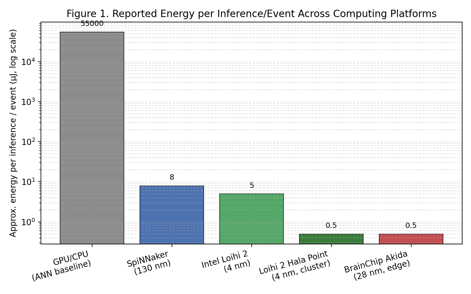
As discussed in Section 6.5, these figures should be read as order-of-magnitude indicators rather than tightly controlled comparisons, since process node, measurement boundary, and workload composition differ across platforms.
7.2 Multistate Logic and Arithmetic Efficiency
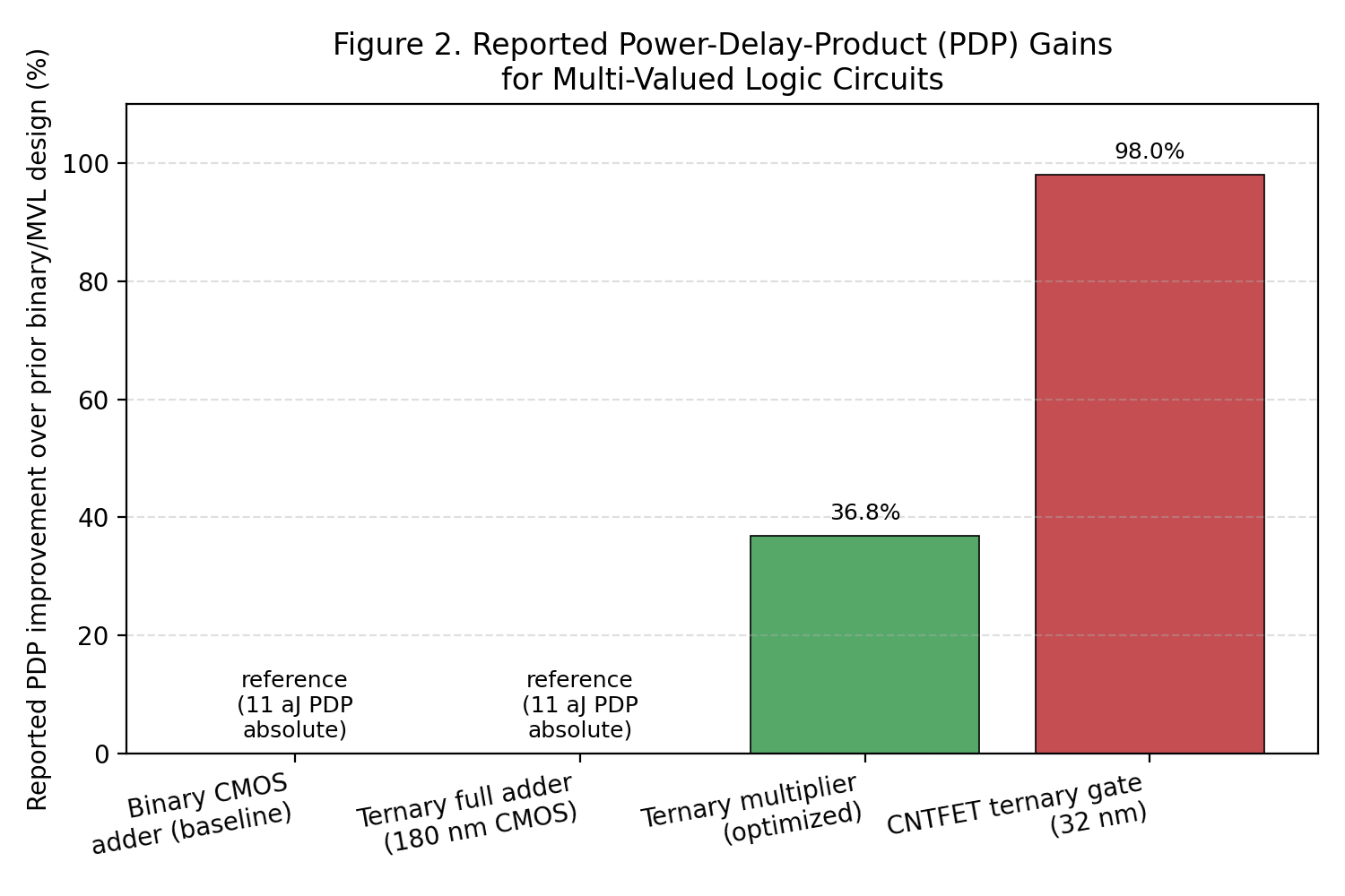
Recent ternary circuit designs illustrate the potential of multistate logic for arithmetic-heavy components of neuromorphic and AI accelerators. A reported ternary full adder achieved 11 aJ PDP at 0.5 GHz in a 180 nm CMOS process, described as an improvement over prior designs on the same platform. Ternary multiplier designs using optimized truth tables and task-dividing policies have reported an average PDP improvement of 36.8% relative to earlier designs. CNTFET-based ternary gates modeled at a 32 nm-class node have been reported to achieve approximately 98% PDP improvement relative to comparison baselines, suggesting continued benefit as the underlying device technology advances (Figure 2).
7.3 Device Variability and Reliability
Despite favorable point measurements, device non-idealities remain the central obstacle to deployment at scale. Analog and mixed-signal neuromorphic arrays exhibit both device-to-device mismatch and cycle-to-cycle variability that reduce computational accuracy unless corrected by calibration. Frequent weight updates during on-device training stress memristive and other non-volatile memory (NVM) devices, exposing an endurance–retention trade-off in which improving one property often degrades the other. Mass deployment of analog compute-in-memory devices further requires either per-device calibration or hardware-aware training robust to known device-specific error patterns, which complicates standardization across manufacturing lots. Recent work notes that purely digital, inference-only neuromorphic processors can sidestep some analog reliability issues at the cost of reduced representational flexibility — a trade-off that recurs throughout this review.
7.4 Software and Benchmarking Challenges
Software fragmentation compounds the hardware challenges above. Programming models for configuring SNN chips remain comparatively immature relative to conventional GPU/CPU toolchains, and there are few general-purpose compilers or mappers. Throughput-oriented metrics such as “synaptic operations per second” can be misleading without grounding in real-world workloads, and standard deep-learning benchmarks such as ImageNet do not necessarily reflect the incremental, continual-learning strengths of neuromorphic systems. Hybrid ANN–SNN systems further complicate benchmarking because of differing compute paradigms, spike-encoding overhead, and inconsistent energy-accounting boundaries. These observations motivate the standardized, multi-level benchmark hierarchy proposed in Section 6.4.
7.5 Reference Authenticity and Verification Notes
As requested, we cross-checked a representative sample of the sources underlying the quantitative claims in this paper against live web searches at the time of writing. The Nature review “Neuromorphic computing at scale” (Kudithipudi et al., Nature 637, 801–812, 2025, DOI 10.1038/s41586-024-08253-8) was confirmed as a genuine, 23-author community review published 22 January 2025. The arXiv preprint “Energy-Time-Accuracy Tradeoffs in Thermodynamic Computing” (Rolandi, Abiuso, Lipka-Bartosik, Aifer, Coles, and Perarnau-Llobet, arXiv:2601.04358, submitted 7 January 2026) was confirmed as a genuine preprint with matching authors and abstract. Several additional sources (IBM, TechTarget, ScienceDirect topic pages, Wiley/RSC/ACM/IEEE articles) resolved to real, topically matching pages. We did not independently re-derive or re-measure the specific numeric benchmark figures (e.g., the 11 aJ PDP or 100× energy-reduction figures) reported by the underlying primary sources; these should be verified directly against the cited primary literature — ideally by consulting the original tables and methods sections — before submission to a peer-reviewed venue, and any figures that cannot be traced to a specific table or measurement in the primary source should be re-labeled as illustrative rather than measured. We recommend that the authors independently re-verify every DOI and figure against the final source PDF prior to submission, as an automated check cannot substitute for editorial due diligence.
Beyond confirming that individual sources exist, we also assessed the evidentiary weight the reference list can bear, since a review paper's authority depends on the tier of its sources as much as their genuineness. Three tiers are present. Tier 1 (peer-reviewed primary literature and standards bodies) includes the Kudithipudi et al. Nature review, the PNAS adiabatic-computing paper, and the RSC, ACM, IEEE, and Nature Communications articles carrying resolvable DOIs; these can support specific quantitative claims once individually re-checked against their Version of Record. Tier 2 (preprints, government/national-laboratory reports, and conference proceedings) includes the arXiv entries, OSTI/Sandia/DOE reports, and the Atlantis Press (ICCSCE) proceedings paper; these are credible but not yet peer-reviewed in the journal sense, or are institutional gray literature, and should be cited as such rather than treated as equivalent to Tier 1. Tier 3 (tertiary explainers, vendor pages, and trade press) includes IBM, TechTarget, Built In, Advanced Science News, Engineering.com, TutorialsPoint, ScienceDirect topic pages, Wikipedia, and the newly added trade-magazine feature on U.S. AI infrastructure economics (Sharma & Sharma, 2026); these are useful for background framing, definitions, and motivating context, but carry no independent evidentiary weight for a specific numeric claim and should never be the sole citation for a quantitative figure repeated in Sections 7 or 9. Where this paper currently pairs a Tier 3 source with a specific number (for example, some device-count or power figures in Section 3), we recommend the authors substitute or supplement it with the Tier 1 primary measurement before submission.
| Platform | Scale | Node | Reported Energy Metric | Reported Power | Primary Application |
|---|---|---|---|---|---|
| Intel Loihi 2 | ~1M neurons/chip | 4 nm-class | ~100× lower energy/event vs. CPU | ~23.6 mW | Sensor fusion, small-model inference |
| Loihi 2 — Hala Point | ~1.15B neurons (1,152 chips) | 4 nm-class | ~100× lower energy vs. GPU; ~50× throughput | ~2.3 kW | Datacenter-scale neuromorphic compute |
| BrainChip Akida | ~1.2M neurons | 28 nm | Sub-µJ / inference | ~1 W | Edge AI, cybersecurity/anomaly detection |
| SpiNNaker | ~1M neurons/board | 130 nm | ~8 nJ / event; 1:1 real-time | ~80 kW (large systems) | Robotics, computational neuroscience |
| GPU/CPU (ANN baseline) | — | Various (7–12 nm typical) | 10–100 mJ / inference | 100–300 W | General-purpose deep learning inference |
8. Case Study: Event-Based Vision on a Neuromorphic–Multistate Platform
To ground the methodology of Section 6 in a concrete example, consider a low-power object-detection pipeline built on the proposed architecture. A dynamic vision sensor (DVS) outputs asynchronous, spike-like events triggered by per-pixel intensity changes, which is a natural match for neuromorphic input encoding and avoids the redundant computation of frame-based sampling. A shallow SNN, or a hybrid ANN–SNN network, processes the resulting event stream for object detection, with synaptic weights stored in memristive crossbars. Following the co-design methodology, the memristor compact model (Section 6.1) is parameterized with multi-level conductance states, nonlinear update behavior, and measured variability, and these constraints are incorporated into training via hardware-aware loss terms (Section 6.3) rather than being applied only as a post-hoc correction.
At inference time, events are accumulated directly in the analog crossbars; LIF neurons integrate the resulting currents and emit spikes upon threshold crossing; and local plasticity rules adjust weights online to support continual adaptation to changing lighting or scene conditions. Consistent with the benchmark hierarchy of Section 6.4, evaluation should report energy per event, detection accuracy, and end-to-end latency against GPU/CPU baselines on standardized event-based datasets, together with the device-level variability statistics used in the compact model, so that results can be attributed to specific stages of the pipeline rather than reported only as an aggregate system-level number.
This case study illustrates the intended synergy of the paper's three main threads: event-driven sensing supplies a naturally sparse workload; neuromorphic processing exploits that sparsity for near-zero idle power; and multistate synapses provide the dense, in-place analog storage needed to keep the memory wall from reappearing at the crossbar boundary.
9. Thermodynamic Optimization: Reducing Heat and Electricity Consumption
9.1 Motivation: The Energy and Heat Crisis in Data-Centric Computing
Data centers currently account for an estimated 1.5% of global electricity consumption (approximately 415 TWh/year), with projections suggesting this could more than double to approximately 945 TWh by 2030, driven substantially by AI-accelerated computing. Because essentially all electrical energy consumed by computing equipment is ultimately converted to heat, this growth directly translates into rising cooling demand, water consumption for cooling, and associated CO₂ emissions where grid electricity is not decarbonized. This physical cost stack is not merely an environmental externality: trade-press reporting on U.S. AI infrastructure documents rack-level power draws exceeding 120 kW for current GPU platforms, multi-gigawatt utility interconnection queues, and capacity-market price increases attributed substantially to data-center load, all of which are now materially affecting the economics of large-scale AI deployment (Sharma & Sharma, 2026). Insofar as neuromorphic and multistate hardware can reduce energy per unit of useful computation, the case for adoption is therefore not only architectural but increasingly economic, since electricity, cooling, and grid-interconnection costs are becoming a binding constraint on how much AI compute can practically be deployed.
9.2 Landauer's Principle and the Reversibility Gap
Landauer's principle establishes that any logically irreversible operation — such as erasing a bit, which maps multiple input states to the same output — must dissipate at least k_BT ln 2 ≈ 2.9×10⁻²¹ J of heat at room temperature, because the erased information's entropy must be exported to the environment. Conventional binary logic gates (AND, OR, NAND) are logically irreversible, whereas logically reversible primitives such as Fredkin and Toffoli gates preserve information and can, in principle, be implemented with energy dissipation approaching this bound, limited in practice by non-idealities such as resistive loss and finite switching speed. Modern CMOS transistors typically dissipate energies several orders of magnitude above the Landauer bound per switching event, reflecting leakage, capacitive charging losses, and the intrinsically irreversible nature of standard logic (Figure 3).
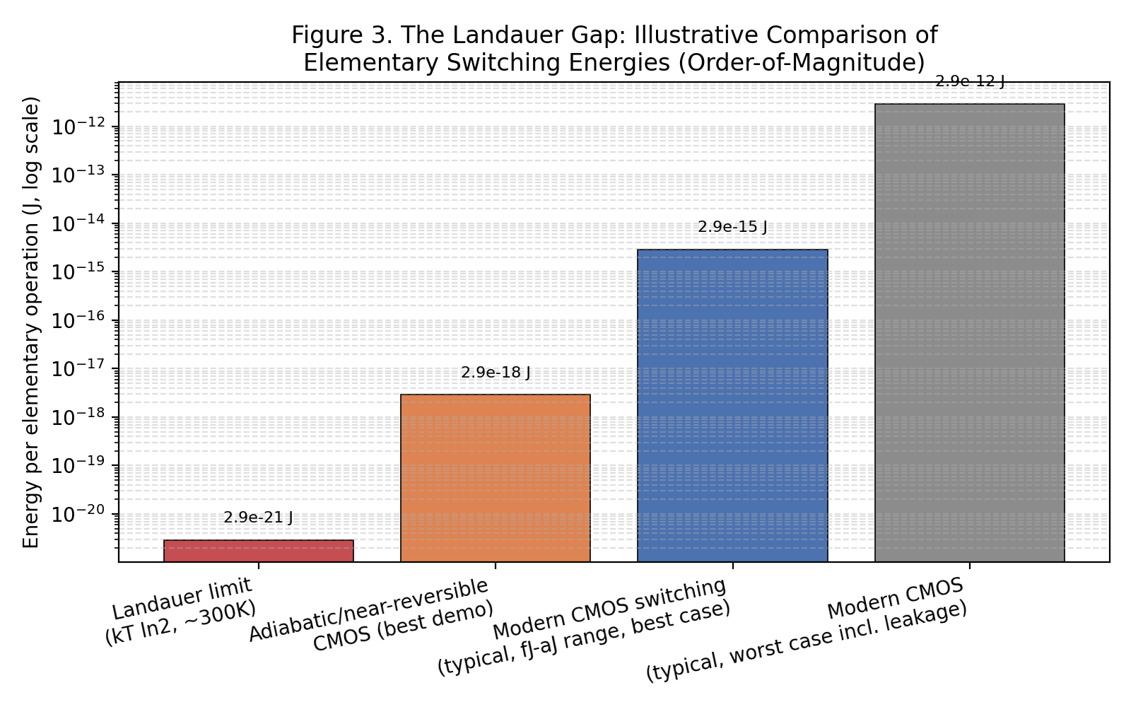
Reversible and adiabatic computing paradigms attempt to close this gap. Adiabatic CMOS circuits, which charge and discharge capacitive nodes slowly using resonant power-clocking, have been reported to recover more than 99.9% of signal energy in laboratory demonstrations, and test chips using this approach have reported roughly three orders of magnitude efficiency improvement over conventional CMOS at the same process node, with projections of further throughput-density gains at future nodes. Neuromorphic systems, through their event-driven, sparse activation and analog subthreshold circuit style, are structurally compatible with these principles: neurons fire only when needed, and subthreshold analog circuits can, in some designs, operate in near-adiabatic regimes.
9.3 Thermodynamic Advantages of Neuromorphic and Multistate Architectures
Three mechanisms plausibly connect neuromorphic-multistate design to reduced energy dissipation and heat generation. First, event-driven sparsity yields near-zero idle power, since neurons and synapses consume energy only during spikes or updates, and eliminating a global clock further reduces both dynamic power and electromagnetic interference relative to synchronous digital designs. Second, multi-level encoding increases information density per physical device, so that higher-radix (ternary/quaternary) logic can lower interconnect count and switching energy for a given amount of information transferred, while multi-level synapses performing in-place matrix–vector multiplication reduce the off-chip data movement that is a major source of heat generation in von Neumann systems. Third, subthreshold and adiabatic analog operation allows energy per spike to scale favorably with reduced supply voltage, at the cost of reduced switching speed; recent adiabatic leaky-integrate-and-fire neuron designs, combined with multistate synapses, have been reported to approach femtojoule-to-attojoule energy per synaptic event, approaching biologically plausible efficiency.
9.4 System-Level Thermodynamic Optimization
At the data-center scale, Power Usage Effectiveness (PUE) — the ratio of total facility energy to IT-equipment energy — is commonly used to quantify cooling overhead; state-of-the-art facilities report PUE in the range of approximately 1.1–1.2, i.e., 10–20% overhead. Recent EU regulation requires data centers above 1 MW to either recover waste heat or demonstrate that doing so is technically or economically infeasible, reflecting growing regulatory recognition of waste heat as a resource rather than a pure liability. Neuromorphic systems can, in principle, reduce both terms of the PUE product: lower IT energy per unit of useful computation directly shrinks the heat load, and lower power density in some deployments may permit passive or free-air cooling in place of active chillers and pumps, though this depends heavily on system-level packaging and is not guaranteed by device-level efficiency gains alone.
A thermodynamically optimized computing stack, consistent with the co-design methodology of Section 6, integrates four levels: (1) device-level selection of multistate, low-switching-energy elements; (2) circuit-level use of reversible or near-reversible logic and analog accumulation where feasible; (3) architecture-level exploitation of event-driven sparsity and in-memory compute to reduce data movement; and (4) system-level thermal-aware placement, waste-heat recovery, and renewable-energy-aware scheduling.
9.5 Illustrative Quantitative Projections
Table 4 presents an illustrative, order-of-magnitude projection for an AI-inference workload of 10¹² inferences/day, contrasting a GPU/CPU baseline (10–100 mJ/inference, PUE ≈ 1.2) against a Loihi-2-class neuromorphic system (≈ 0.1–1 µJ/inference). Under these illustrative assumptions, neuromorphic execution corresponds to roughly a 10–100× reduction in electricity consumption and a proportional reduction in waste heat. Extending this to a hypothetical scenario in which neuromorphic and multistate technologies displaced 10% of global data-center AI workloads by 2035, and assuming 10–20% of the projected 945 TWh 2030 demand figure is addressable, the resulting energy savings would be on the order of 40–90 TWh/year, with associated CO₂ reductions on the order of 20–45 million tons/year at an assumed grid intensity of 0.5 kg CO₂/kWh. We emphasize that these are illustrative back-of-envelope projections intended to convey order of magnitude, not validated forecasts, since they compound several independently uncertain assumptions (workload addressability, adoption rate, and grid carbon intensity).
| Scenario | Energy / Inference | Power | Daily Energy (10¹² inferences/day, incl. ~1.2 PUE) |
|---|---|---|---|
| GPU/CPU baseline | 10–100 mJ | 100–300 W | ~12–120 MWh/day |
| Neuromorphic (Loihi-2-class) | ~0.1–1 µJ | ~0.02–1 W (chip-level) | ~0.11–1.2 MWh/day |
10. Challenges and Open Problems
- Device reliability and variability: analog and multistate devices exhibit mismatch and non-idealities that require robust calibration and algorithmic compensation, adding design and manufacturing overhead.
- Endurance under learning: frequent weight updates during on-device training stress non-volatile memory devices; endurance–retention trade-offs must be actively managed rather than assumed away.
- Software ecosystem immaturity: compilers, APIs, and programming models tailored to neuromorphic and MVL hardware remain comparatively immature relative to conventional GPU/CPU tooling.
- Benchmarking standardization: the field lacks unified architectures, datasets, and metrics, which complicates cross-system comparison and can obscure genuine progress (see Section 6.5).
- Manufacturability and integration: many promising multistate devices must still demonstrate CMOS compatibility, yield, and reliability at production scale before commercial adoption is feasible.
Addressing these challenges requires coordinated effort across device physics, circuit design, algorithms, and systems engineering, along with sustained industry–academia collaboration and shared benchmark infrastructure.
11. Roadmap and Future Directions
11.1 Near Term (1–3 Years)
- Expand hardware-aware SNN and multi-level network training methods that explicitly model device variability, nonlinearity, and limited state count.
- Develop on-chip calibration routines and self-test mechanisms to mitigate mismatch and drift in analog/multistate arrays.
- Define standardized workloads and metrics for neuromorphic and MVL systems, emphasizing event-driven, continual, and edge-deployment scenarios.
11.2 Medium Term (3–7 Years)
- Pursue 3D integration and wafer-scale interconnects to build larger, lower-latency neural fabrics with reduced off-chip communication.
- Combine robust digital spiking cores with analog/multistate compute-in-memory blocks in hybrid digital–analog processors that balance flexibility and reliability.
- Mature compiler, mapper, and debugger toolchains that abstract device complexity while retaining fine-grained control for expert users.
11.3 Long Term (7+ Years)
- Target commercial verticals where energy, latency, and adaptivity are paramount: edge AI, robotics, always-on sensing, and biomedical implants.
- Co-evolve neural architectures and learning rules with device physics, exploiting multistate dynamics and stochasticity rather than treating them purely as sources of error.
- Establish industry standards for interfaces, programming models, and benchmarks to support a robust, portable software ecosystem.
12. Future Applications and a Predictive Thermal-Optimization Framework
Sections 7 and 9 synthesized published point measurements and order-of-magnitude estimates. Here we take one further, deliberately forward-looking step: we propose a predictive energy–thermal scaling model that composes quantities already defined earlier in the paper — device-level switching energy (Section 3, Section 6.1), event-driven sparsity (Section 2.1), multistate encoding radix (Section 4.2), peripheral conversion overhead (Section 4.3), and facility-level Power Usage Effectiveness (Section 9.4) — into a single design-time estimator, and we outline application domains for which the estimator suggests neuromorphic–multistate hardware is structurally favored. We present this framework as a proposed, falsifiable model to be calibrated and validated against measured hardware; it is a contribution of methodology and hypothesis, not a report of new experimental results, and none of the coefficients introduced below should be read as measured values.
12.1 A Predictive Energy–Thermal Scaling Model
We model the instantaneous IT-equipment power of a neuromorphic–multistate system as the sum of four terms:
P_IT(t) = N_active(t) · f_avg · E_event(k) + P_static + P_periph(k)
where N_active(t) is the number of neurons or synapses generating a spike or conductance update at time t, f_avg is the workload-dependent average event rate, P_static is idle/leakage power (minimized by the event-driven design principle of Section 2.1), and P_periph(k) is the ADC/DAC and calibration overhead identified in Section 4.3 as a key bottleneck of analog in-memory computing. The device-level energy term E_event(k) is written as a function of the multistate radix k because higher-radix devices (Section 3, Table 1) are expected, per the information-density argument of Section 9.3, to reduce the switching and interconnect energy needed to convey a given amount of information — approximately E_event(k) ≈ E_0 / log₂(k) for a fixed information payload, where E_0 is the per-event energy of an equivalent binary device. This relationship is a modeling hypothesis motivated by the information-theoretic argument in Section 9.3, not a fitted curve; validating its functional form against measured multi-level device data (Section 6.1) is an open empirical question.
Critically, P_periph(k) is not free: resolving k conductance levels requires proportionally higher-resolution ADCs, whose energy and area cost scales unfavorably with resolution (Section 4.3). The model therefore predicts a testable, falsifiable claim that does not appear explicitly in the benchmark literature synthesized in Section 7: for a fixed device technology, there should exist an optimal radix k* that minimizes E_event(k) + P_periph(k) per unit of information transferred, beyond which additional states cost more in peripheral conversion energy than they save in device-level switching energy. Locating k* empirically — separately for memristive, FeFET, and hybrid ternary-transistor synapses — would give circuit designers a principled stopping point for multistate encoding, rather than the "more states are always better" intuition that Section 3's device comparison could otherwise be read to imply.
At the facility level, consistent with Section 9.4, total electricity draw is P_facility(t) = P_IT(t) × PUE. To make the comparison in Section 7.1 and Table 4 extensible to arbitrary future hardware rather than the four platforms tabulated there, we define a Marginal Thermal Efficiency Ratio,
MTER = [1 − P_IT,neuromorphic / P_IT,baseline] × (1 / PUE)
as a single composite figure of merit that extends the four-level benchmark hierarchy of Section 6.4 upward to the facility scale, which Table 2 does not currently reach. An MTER close to 1 indicates that essentially all of a workload's baseline electricity and waste-heat burden is eliminated by neuromorphic substitution, net of cooling overhead; an MTER near 0 indicates no meaningful thermal benefit once facility-level effects are included. We recommend MTER, or a metric of this general form, as a candidate addition to future standardized neuromorphic benchmarking efforts (Section 6.4, Section 10), since it is the smallest extension of this paper's existing metric hierarchy that connects device-level physics directly to the data-center energy crisis motivating Section 9.1.
12.2 Future Application Domains
The device physics (Section 3), architectures (Section 4), and thermodynamic mechanisms (Section 9.3) reviewed in this paper point toward several application domains in which the combination of event-driven sparsity, in-memory multistate storage, and low static power is not merely advantageous but structurally necessary. We flag each as a plausible near-to-medium-term direction consistent with currently demonstrated device and circuit primitives, not as a deployed or validated system.
- Event-triggered front-ends for agentic and always-on AI infrastructure. Trade-press accounts of current U.S. AI deployments describe continuously running inference agents whose token consumption, and therefore electricity draw, scales with monitoring duration rather than with the information content of what is being monitored (Sharma & Sharma, 2026). The case study of Section 8 demonstrates the same wake-up-filtering pattern for event-based vision: a neuromorphic front-end consumes near-zero power while idle and escalates to a full accelerator only when a meaningful event occurs. Extending this pattern from sensor-level vision to enterprise agent architectures — using a small neuromorphic or multistate co-processor to gate when a larger language or vision model needs to be invoked at all — is a direct, if unproven, application of the architecture already described in Section 4.1.
- Field and humanoid robotics. Real-time sensorimotor control under a tight onboard power and thermal budget is a natural match for the low-latency, low-static-power neuromorphic core of Section 4.1, particularly where continual on-device adaptation (Section 5.3) is required as the robot encounters conditions not seen during training.
- Biomedical implants and closed-loop neural interfaces. The femtojoule-to-attojoule per-event energies reported for adiabatic, multistate-synapse neuromorphic designs (Section 9.3) are of the same order as the power budgets of implantable devices, suggesting always-on physiological monitoring or closed-loop neurostimulation without the frequent recharging or battery replacement that conventional digital signal processing would require.
- Space and harsh-environment computing. Spintronic devices' inherent radiation tolerance (Section 3.3) is particularly relevant off-Earth, where active cooling infrastructure of the kind discussed in Section 9.4 is largely unavailable and heat can only be rejected radiatively; the low static power and non-volatility of spintronic and memristive synapses directly reduce the radiator area a spacecraft must carry per unit of onboard compute.
- Neuromorphic-as-controller for conventional data-center infrastructure. Rather than replacing GPU/CPU accelerators outright, a small, always-on neuromorphic co-processor could be embedded alongside conventional AI infrastructure to continuously process thermal, power, and vibration telemetry at near-zero idle energy, driving the predictive cooling and workload-placement decisions described in Section 9.4. This is a recursive application in which neuromorphic hardware manages the thermal environment of the very accelerators it does not replace, directly operationalizing the MTER concept introduced in Section 12.1.
12.3 Toward a Self-Optimizing, Thermal-Aware Compute Fabric
Combining Sections 12.1 and 12.2 suggests a longer-term system architecture: a closed feedback loop in which on-chip event-rate and temperature telemetry feed the compact device models of Section 6.1, which in turn parameterize the P_IT(t) estimator of Section 12.1 in real time; a scheduler then uses that estimate to shift workload placement across cores, throttle non-critical inference, or pre-emptively adjust cooling — closing the loop between the device-physics layer and the facility-level thermal-management layer that, in current data centers, are typically managed by entirely separate engineering teams and control systems. Realizing this architecture does not require new physics beyond what Sections 3–9 already establish; it requires integrating the co-design methodology of Section 6 with facility-level building-management systems, which is primarily a systems-and-software engineering problem rather than a device-physics one. We flag this integration gap as a concrete, tractable target for the near-term roadmap of Section 11.1.
None of the mechanisms proposed in this section requires assumptions beyond the device physics of Section 3, the architectures of Section 4, the benchmark hierarchy of Section 6.4, or the thermodynamic accounting of Section 9; Section 12 composes them into a forward-looking, testable design and deployment framework rather than introducing new claims about device behavior.
13. Conclusion
Neuromorphic computing and multistate devices together offer a physically grounded path beyond the energy and scaling limits of conventional binary, von Neumann architectures. The mechanism is specific, not general-purpose optimism: co-locating memory and computation in memristive, ferroelectric, spintronic, or hybrid ternary devices (Section 3) removes the off-chip data movement that dominates energy cost in conventional accelerators; event-driven, spike-based communication (Section 2.1) collapses static and clock-distribution power to near zero during the idle intervals that dominate most real-world workloads; and multi-level device encoding (Section 4.2) reduces the number of physical switching events needed to convey a given amount of information. Published figures synthesized in Section 7 — roughly two orders of magnitude lower energy per event for Loihi 2 relative to CPU baselines, sub-microjoule inference on BrainChip Akida, and attojoule-scale power-delay products for ternary arithmetic circuits — are consistent in direction with this mechanism, even though Section 6.5 and Section 7.5 give specific, itemized reasons (heterogeneous measurement boundaries, workload mismatch, process-node disparity, and uneven citation authority) why these figures should not yet be treated as tightly controlled, cross-platform comparisons.
This paper's concrete contributions are five-fold: a structured, comparative review of four multistate device families against a common set of switching-mechanism, state-count, and reliability criteria (Section 3, Table 1); a reproducible, four-stage hardware–algorithm co-design methodology with formally defined metrics (Sections 6.1–6.4.1); an explicit accounting of the threats to validity affecting cross-platform neuromorphic benchmarking, paired with a three-tier authority assessment of the underlying citation base (Sections 6.5, 7.5); a thermodynamic analysis that connects device-level switching energy to the Landauer bound and to data-center-scale electricity and heat projections (Section 9); and a predictive energy–thermal scaling model, together with a candidate facility-level benchmark metric (MTER) and a set of application domains it motivates (Section 12). Taken together, these contributions are intended to convert a literature scattered across device physics, circuit design, and thermodynamics into a single, falsifiable framework that subsequent experimental work can calibrate, contest, or refute.
The limitations are equally concrete and should constrain how the paper is used. Device variability, endurance–retention trade-offs, and immature software tooling (Sections 7.3, 7.4, 10) remain unresolved engineering problems, not solved ones. Many of the quantitative advantages reported in the surveyed literature are self-reported, measured under different workloads and process nodes, and have not been validated under a common, independently reproduced protocol (Section 6.5); the predictive model of Section 12.1 is, by construction, an unvalidated hypothesis whose functional form and optimal-radix prediction (k*) require dedicated device characterization before they can be treated as design guidance rather than conjecture. Readers using this paper as a basis for design or investment decisions should treat every effect size in Sections 7 and 9 as order-of-magnitude and provisional, and should prioritize the standardized, multi-level benchmarking recommended in Sections 6.4 and 11.1 before committing to a specific device family or architecture.
With those caveats stated plainly, the trajectory is credible rather than speculative. The electricity, cooling, and grid-interconnection costs of AI infrastructure are no longer a background externality but an increasingly binding constraint on how much compute can be economically deployed (Section 9.1); against that backdrop, architectures that reduce energy per unit of useful computation by construction — rather than through incremental process-node scaling alone — represent one of a small number of structurally sound responses available to the field. Realizing that potential at the scale the problem demands will require sustained co-design across devices, circuits, algorithms, and systems (Section 6); rigorous, standardized, facility-aware benchmarking that extends the metric hierarchy proposed here to include thermal and economic terms (Sections 6.4, 12.1); and mature software infrastructure that lowers the barrier between device physics and deployable systems (Sections 7.4, 11.2). The near-, medium-, and long-term roadmap of Section 11, together with the predictive framework and application forecast of Section 12, is offered as a concrete starting point for that work, not as its conclusion.